|
|
Post by gjaky on May 18, 2017 1:25:57 GMT -5
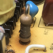
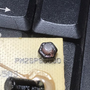
During the work with the ULTIMATE VNB-DB I managed to measure the output speed of the VNB. The VNB was modified so the whole input opamp circuit is bypassed, and Q19 was directly driven by my pulse generator. Q19 was replaced with a faster transistor, a 2SC3613 (3,5GHz). On the picture the K output is shown, with no apparent load, only the FET probe (~1pF), the output is 60Vpp, the rise time is 3ns on picture. After correcting this with the self rise-time of the generator and the scope we get 2.6ns rise time out of the VNB, that roughly equals 135MHz clean sine bandwidth at -3dB roll off. For reference the VPA13 video pack is rated at 130MHz bandwidth, but the rise time is typically 3ns at 50Vpp output, the difference may not seem too much, but in fact it is... I'd like to note here that one should NOT confuse these numbers with pixel clock and so on, the rise time have real meaning, which is well defined. So far this is the fastest rise time out of a CRT driver I've ever seen. 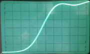 |
|
|
|
Post by barclay66 on May 18, 2017 3:16:14 GMT -5
Hi,
Quite some nice achievement! Just for curiosity:
The 2SC3613 is quite big. How did You fit it onto the SMD pads? Wouldn't a SMD type be even better (less capacitance/inductance)? I thought of using the BFG35 (4 GHz, see datasheet). What do You think? As far as I can see, Q12 can be let alone as it hasn't any influence on bandwidth, correct?
Regards, barclay66 Attachments:BFG35.pdf (283.69 KB)
|
|
|
|
Post by gjaky on May 18, 2017 6:06:12 GMT -5
I also have BFG135 which is 7GHz, but I have problem to source them in quantities, while I have a lot of the 2SC3613 already. In an event of failure the maximal current is 200mA in the cascode circuit, butthe BFGs are rated to 100-150mA collector current so it is noto nice, although it can work in normal applications. The pinout of the 2SC is not ideal, the base is floating in the air, but it is tied to the daughterboard anyway. 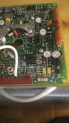 Q12 isn't really limiting bandwidth indeed since most of the time it is working in common base mode which is the highest bandwidth mode a transistor can be used. |
|
|
|
Post by barclay66 on May 18, 2017 7:05:18 GMT -5
Q12 isn't really limiting bandwidth indeed since most of the time it is working in common base mode which is the highest bandwidth mode a transistor can be used. Hi, I don't know if I understand the circuit around Q19/Q12 correctly, but as it seems Q12 doesn't carry the video signal at all. It only modulates the amplified video with auxiliary signals (coming from a slow MC34072). Another candidate for Q12 could be the 2SC5551 (30V, 300mA, 600mA peak, 1.3W, 3.5GHz)... Regards, barclay66 |
|
|
|
Post by gjaky on May 18, 2017 8:50:01 GMT -5
Q12 isn't really limiting bandwidth indeed since most of the time it is working in common base mode which is the highest bandwidth mode a transistor can be used. Hi, I don't know if I understand the circuit around Q19/Q12 correctly, but as it seems Q12 doesn't carry the video signal at all. It only modulates the amplified video with auxiliary signals (coming from a slow MC34072). Another candidate for Q12 could be the 2SC5551 (30V, 300mA, 600mA peak, 1.3W, 3.5GHz)... Regards, barclay66 Q12 does carry high frequency video signal between its collector and emitter. All parts tied between the +/-85V rails carry high frequency signals: Q12, Q17, Q19, Q21, R13, R28 et al. Q12 is set on a specific bias voltage against Q19, which can be treated as a DC signal from RF viewpoint, therefore it appears to be working in common base configuration most of the time just like Q17 and Q21. The voltage difference between their (Q19, Q12) emitters is transformed to current through R9 and the parallel peaking network, then this current is "forced" through all these series tied components (because there is no other path to flow for this current) and will result in the useful video signal as a voltage drop on R28 an R13. It is all very simple isn't it?  As for transistor quality Q21 has the most impact on bandwidth as it is used as a phase inverter and as such it is influenced by the Miller effect. Theoretically the input of the VNB could be fully symmetrical as well by driving Q12 and Q19 simultaneously, but also an other approach could be to omitt Q12 completely and do biasing through Q17. Either way the output bandwidth will be limited mostly by the time constant of the RC network formed by the work resistors (R13, R28) and the grand sum of all (including parasitic) capacitance those are present on the collectors of Q17 and Q21. With carefully adjusted peaking networks some of those capacitances can be compensated, but certainly not all and not perfectly. |
|
|
|
Post by barclay66 on May 18, 2017 9:24:40 GMT -5
Thank You for this insight. I always thought that anything beyond 20kHz or digital stuff was a bit like voodoo because of effects that can be ignored at LF and this circuit surely reassures me on that. ;-)
|
|
|
|
Post by stridsvognen on May 18, 2017 12:11:44 GMT -5
I would be super curious to see how the original transistor on Q19 measures.
I think i have had all of the BFG transistors on Q19, and know MP uses the BFG 97, it always seems to compromise something replacing it, so i stick to the original setup, but im ready to try something new.
A good original neckboard, with the input peaking and FB3 removed, and the gain on the input lowered is super well behaved to 360Mhz pixel clock, both to gain and bandwidth.
Im wondering if it would make sense to scope different input levels, a bit like simulating a 20-60-100% IRE, see if it responds consistent to different levels.
|
|
|
|
Post by gjaky on May 18, 2017 14:32:44 GMT -5
You are partly right about Q19. But the 2SC3613 was actually designed to be high resolution video driver transistor, while the BFG line is a general purpose RF transistor. Also 2SC3613 was used in high volumes in all NEC CRT projectors since debut of the PG line, and NEC projectors were always praised by their excellent color reproduction. Also take a look at the curves I collected for you. it shows the current gain linearity of the transistors, basically these showing how difficult load the input of the transitor look like when driving. Philips (NXP) RF transistors generally don't fare very well in this area. As you can see the BFG's current gain almost doubles with output current, while the 2SC is almost completely flat all the way. Also as I already mentioned the BFG transistors are specified at somewhat lower currents, while they can work of course on the VNB, but they are less robust for sure, for example the green neckboard can easily driven at 150mA current, which is 1,5 times what the BFG97 is rated at... 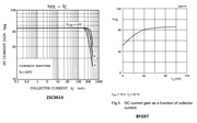 Also I tried to test the original Q19 in the same neckboard but it did not survive the soldering as it produced some quite nasty overshoot paired with slow (5ns) rise time. Yesterday I also tested one of my favourite old M9000 neckboard the same way, but with its original 2N5109 transistor there, and that board also produced rise time around 3.5ns (after correction this equals to 3.2ns, ~110MHz). Playing with Q19 can only yield a few hundred picoseconds in rise time back and forth I admit, but that is still more than nothing. |
|
|
|
Post by gjaky on Jul 10, 2017 14:16:24 GMT -5
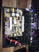
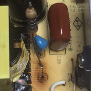
The first set of ULTIMATE VNB-DB is now working! 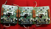 |
|
|
|
Post by stridsvognen on Jul 10, 2017 16:25:17 GMT -5
Thats some seriously nice looking work right there..
|
|
|
|
Post by mastertech on Jul 10, 2017 20:38:15 GMT -5
Who is doing the testing and can we expect to hear some responses?
|
|
|
|
Post by gjaky on Jul 11, 2017 2:17:45 GMT -5
Who is doing the testing and can we expect to hear some responses? A few months ago I sold all my NEC projectors and made a deal on a VDC 9500LC ULTRA, so I could perform some tests. At the new owner the boards will be installed by a calibrator guy, but he is not a member here. I guess I'll get some feedback so I can share it  |
|
|
|
Post by gjaky on Dec 18, 2017 17:57:49 GMT -5
Hm.. I forgot to update the topic. So the boards were installed some time ago, and by a fortunate coincidence I also could check out the machine in person after installation. The installator guy's first impressions were these: -super clean picture.
-nosiefree with lots of fine details, even when looking direct into the tube one can’t detect any noise.
-blacker black, whiter white, much finer color shades.
-more 3d.
-super sharp.
that’s a hell of an upgrade...
I have slightly tuned the circuit further, here is a frequency response plot of the latest version. It remains flat within +/-1.5dB up until ~550MHz, the -3dB point is around 610MHz. 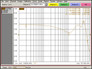 |
|
|
|
Post by Casethecorvetteman on Dec 21, 2017 6:30:57 GMT -5
Well Gábor with this work done, im wondering how you'd go making it possible for me to throw a set of P19LUG tubes into an XG, getting a decent set of working yokes would be the only issue i reckon.
My XG has an issue at the moment where it loses convergence and amplitude as it warms up, i havent had a chance to pull it down and open it up yet, but ive got the impression being an NEC itll be capacitors that are failing. Hopefully theyre not leaking and killing boards...
|
|
|
|
Post by gjaky on Dec 21, 2017 7:49:26 GMT -5
It would be pretty straightforward to do that tube swap. The key is to collect the right yokes together those match to the XG electronics and can fit on a 9" tube. The deflection yoke is the most important to get matched, that should be a Sony G90 yoke or maybe a 1292. The rest is machine work and find out the proper wiring of the coils.
|
|