nashou
Unmoderated Off Topic
Tech in Training.....
Posts: 1,239 
|
Post by nashou on Mar 28, 2016 20:42:58 GMT -5
Well you are asking me a question that is difficult to answer. I know you looked at some schematics of a similar amp to come up with the 1s1555 but I have not seen this schematic. So I have no basis for that conclusion. I will also add that the circuit will not run without the output transistors installed so that would not be a conclusive test. You could put anything in the diode places without the outputs it would not do a thing. Edit: well yes, you could see if the other channel works. Well, the press release for this amp says the amp section is the similar to the A-1 we worked on before. And the Yamaha expert from france( Clinic-Audio) says he thinks its a clone of the CA-810 or 510 etc. To be honest most of the yamaha amps have a similar layout to me at least, but i'm not as fluent in these matters as you guys are  . Hopefully Patrice( Clinic-Audio) will get some info back from his contact in Japan. Hopefully a schematic at least ! I'll put the parts in, I need to at some pint anyhow. I wish I had a variac transformer  Edit: I have two sets of the complimentary output transistors, so I could just grab a hold of my balls and go ! Since i have a back up pair  |
|
nashou
Unmoderated Off Topic
Tech in Training.....
Posts: 1,239 
|
Post by nashou on Mar 28, 2016 21:44:49 GMT -5
One other thing, Some replacement resistors I have are 1/4 watt. I think the originals are 1/2 watt. The 1/4 watt ones seem to have thinner leads.
Hope this won't be an issue at this point.
|
|
|
|
Post by mastertech on Mar 28, 2016 21:54:09 GMT -5
If the originals were 1/2 watt then you must use that or larger. You cannot use 1/4 in place of 1/2 watt.
|
|
nashou
Unmoderated Off Topic
Tech in Training.....
Posts: 1,239 
|
Post by nashou on Mar 28, 2016 22:05:45 GMT -5
How can I tell? The Original resistors are smaller than the 1/2 watts I have of the same value for replacement. It's just the leads seem thinner n the 1/4 watt ones.
The 1/4 watt replacements are closer to the physical size. Also my replacements are metal film, some of these are carbon's.
Nashou
|
|
|
|
Post by mastertech on Mar 28, 2016 22:08:24 GMT -5
When I look at the attached schematic from the A-1 to try to compare, I believe the red circled diodes are possible ones of your bad ones. If you look at the legend in that pic you see that all the basic diodes are 1s1555, as you believe but there are a couple zener diodes in there (HZ6C). Can you be absolutely sure that none of your bad diodes are zeners?  |
|
nashou
Unmoderated Off Topic
Tech in Training.....
Posts: 1,239 
|
Post by nashou on Mar 28, 2016 22:17:30 GMT -5
I'm pretty sure, I found a zener diode marking on another part of the board. However I need to double check under the good channel diode where the board on the bad side is badly burned.
|
|
|
|
Post by mastertech on Mar 28, 2016 22:23:13 GMT -5
How can I tell? The Original resistors are smaller than the 1/2 watts I have of the same value for replacement. It's just the leads seem thinner n the 1/4 watt ones. The 1/4 watt replacements are closer to the physical size. Also my replacements are metal film, some of these are carbon's. Nashou It is your guess. I see the A-1 schematic or parts list does not even give resistor wattage's. Poor diagrams. |
|
nashou
Unmoderated Off Topic
Tech in Training.....
Posts: 1,239 
|
Post by nashou on Mar 28, 2016 22:33:37 GMT -5
I could stack two 1/4 watt resistors of twice the value to get the same results as a half watt right?
|
|
|
|
Post by mastertech on Mar 28, 2016 22:44:40 GMT -5
I would not advise that.
|
|
nashou
Unmoderated Off Topic
Tech in Training.....
Posts: 1,239 
|
Post by nashou on Mar 28, 2016 22:51:45 GMT -5
Ok, I'll just use something as close as I have , I series would work better I take it if I use the 1/2 watt .
|
|
nashou
Unmoderated Off Topic
Tech in Training.....
Posts: 1,239 
|
Post by nashou on Mar 29, 2016 7:27:01 GMT -5
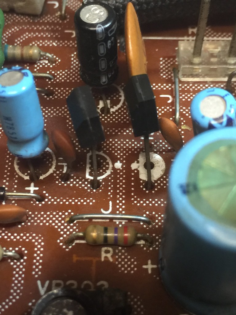
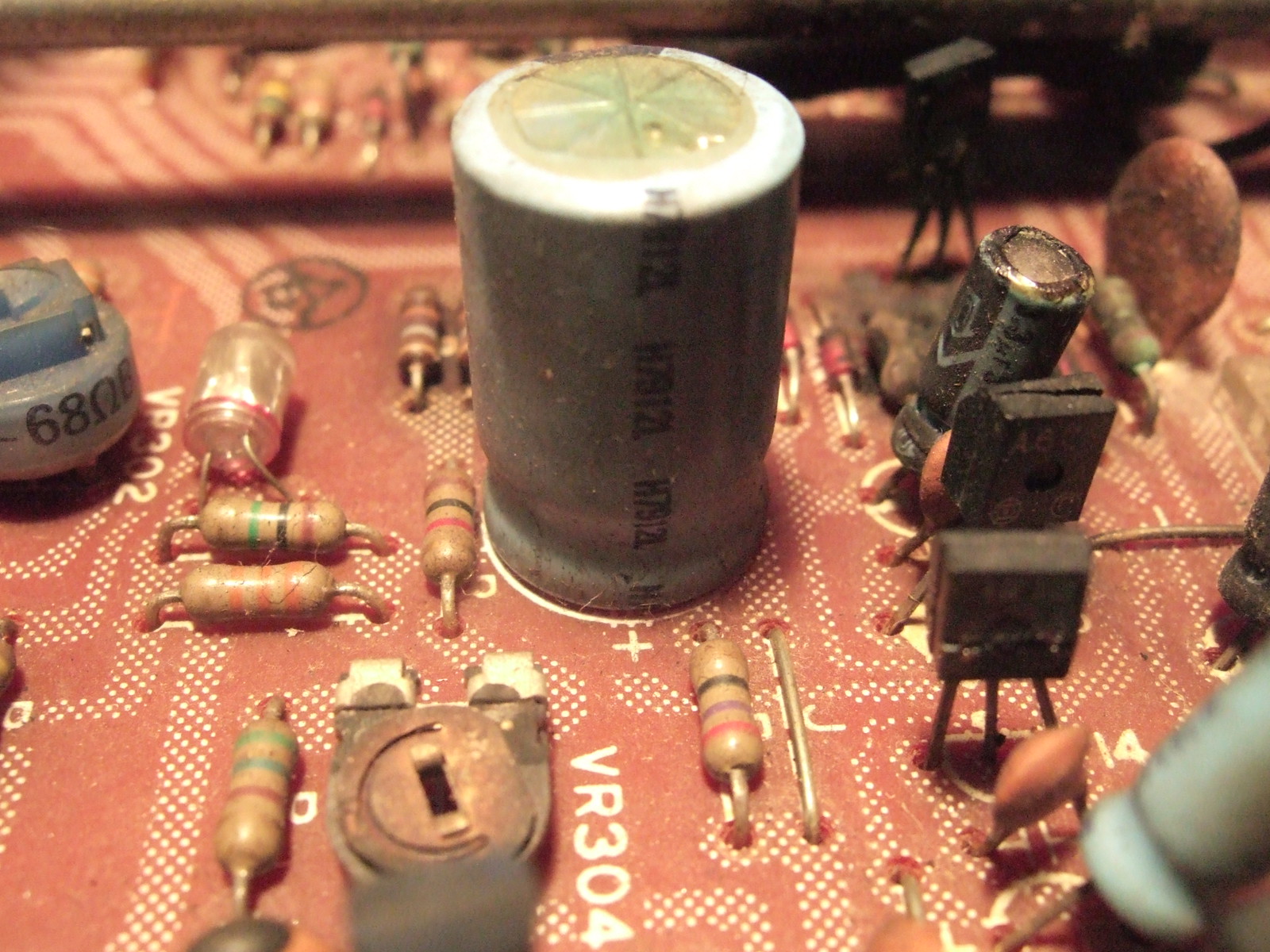
Ok , I really wish I had schematics. Something is strange here. Either the silk screen is wrong or some one worked on this before and they are who caused the failure. Here is a pic of the channel that was not damaged. look at the transistors position relative to the silk screen. They are back wards it seems . I would thing the side with the Part number faces the same as the silk screen? On the bad channel i put them as I think they should go according to the silk screen, but now I am having doubts. Ugh !!!!!!!!!!! And if you look at the other transistors placement on the picture of the entire board in another post they are oriented to the silk screen. Also the 2SC1213A i bought new have a rounded back not flat like the one on the left below(2SC1213A) I'm so confused !!! Below, the good channel, fronts facing opposite the silk screen.
Below on the bad channel before removal , you can see they too do not face the way the silk screen is, the text is facing the camera if you can't make it out.

Here you can see some other TR's in the correct orientation to the silk screen.  ? ?

Although I did find underneath the braided cables more of those squarish transistors also facing the opposite of what you'd think they should go. hmmmm.....
|
|
nashou
Unmoderated Off Topic
Tech in Training.....
Posts: 1,239 
|
Post by nashou on Mar 29, 2016 13:15:40 GMT -5
I investigated how the Base, collector and emitter of the existing PNP's and NPN's pins were tied to on the PCB and made the same tie in for the new parts on the bad board. It was late and my brain was on over load by that time. I also removed the Speaker switch board that the switch is on and disassembled the stuck switch and put it back together as it should be. I guess it jumped out of the tracks it is suppose to travel on to allow it to stay in or out. I also tired to straighten out the Volume control post and cleaned all switches with contact cleaner to flush out the WD-40 I originally use to get the heavy crap off. All left now is to instal the board so I can line up the output transistors onto the center frame rail it uses as a heat sink. That will happen after work or tomorrow. I hope the diodes work. I do not think any that are bad are Zeners. If it reusables the CA-810 I did not see any in that circuit, but if it resembles the A-1 then It might be an issue. But then again the Zeners I found on the A-3 are not in the section area near the blown parts. Hopefully Patrice will get info form his Japan contact  . Athanasios |
|
nashou
Unmoderated Off Topic
Tech in Training.....
Posts: 1,239 
|
Post by nashou on Mar 30, 2016 14:52:58 GMT -5
Ok Tried to power it up and the fuse in the transformer blew. Uh oh I know something was up. SO I figured well to figure this out i'll have to take a chance to burn something up again.
So I didn't have any fast blow 5 amp fuses so I used a slow burn 4 amp I have in the step down transformer . Plugged in the A-3 crossed my fingers, pushed the power button, and after a second the A-3's fuse blew, CRAP!!!
I then looked at the board and nothing looked bad. further investigation proved that the two output transistors blew again. Tested most of the parts on that section that were burnt from before and they all tested ok.
So how should I proceed?
I was thinking of pulling the good channels output transistors out and measuring the pads they attach to and compare along the way going backward . I did a preliminary test and right off the bat they are not equal.
Ugh !!!!
This is definitely a challenge but I want to see this live again !!!
Nashou
|
|
|
|
Post by mastertech on Mar 30, 2016 17:15:27 GMT -5
Yes, compare readings to good channel.
|
|
nashou
Unmoderated Off Topic
Tech in Training.....
Posts: 1,239 
|
Post by nashou on Mar 30, 2016 17:51:02 GMT -5
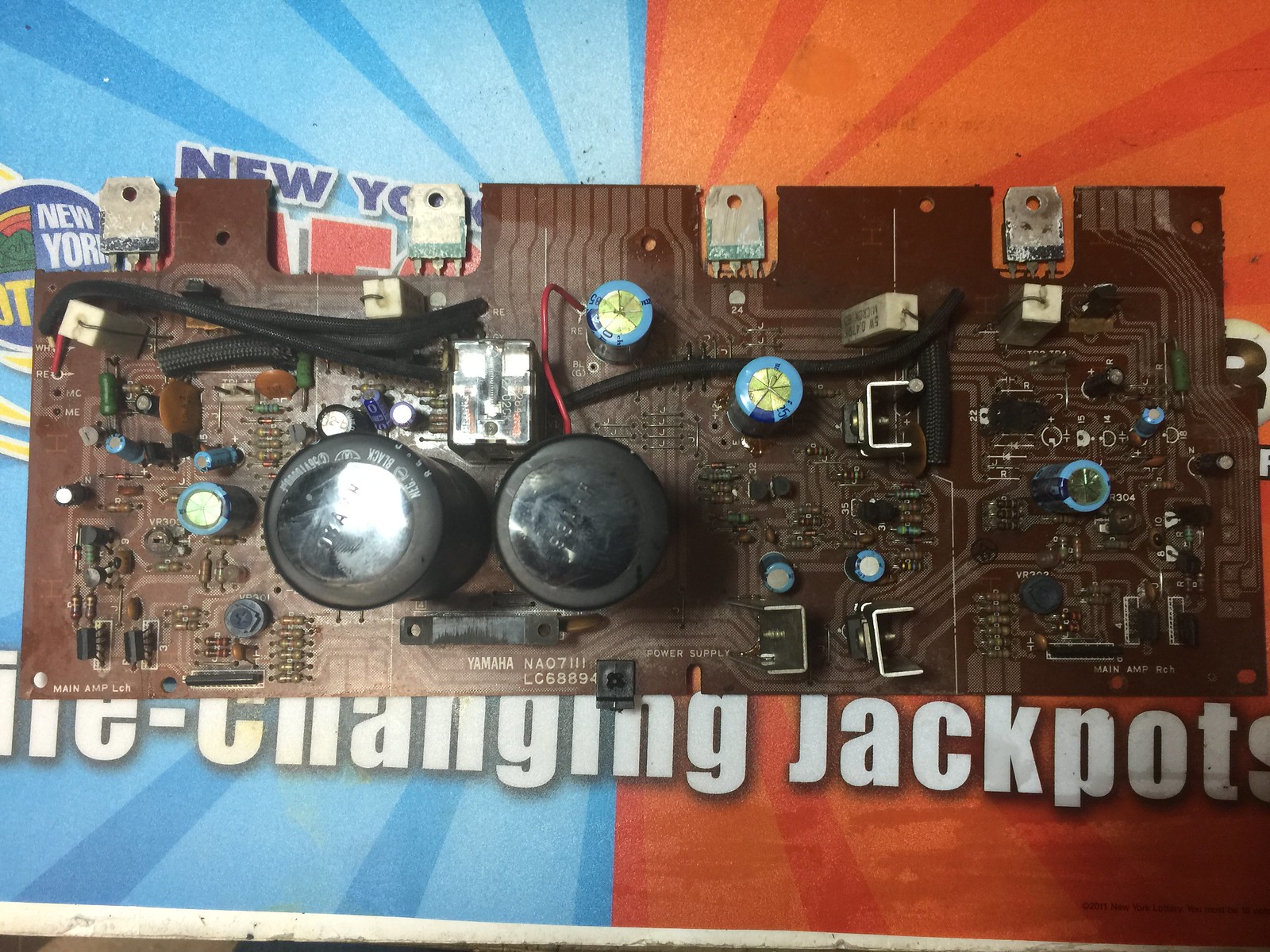
Most of the parts that were burnt were from the section of the 718 transistor compared to the 688 transistor . Could it be possible that something on that section? What is hard to compare is both sections are not layed out the same on the board. They look completely different.
|
|