Post by minisundae on Jan 2, 2020 8:14:21 GMT -5
Hi all-
I have a L42X01A TV with a dead power supply - it blew the main fuse and I couldn't measure any shorts, but when I replaced the fuse, it blew again and left a mark between the drain and source of Q3 - which is in the PFC stage of the SMPS.
The PFC stage uses a NCP1653A which drives three 2SK3658 NMOS (Q1, Q2 and Q3) which has the drain and the source connected in parallel; the gate connection is different:
The gate of Q1 and Q2 are driven in parallel by a transistor (Q8) - it's either a PNP or an NPN; the emitter and collector are connected between Vcc and the gates of Q1, Q2.
On the other hand, Q3 is driven by a PNP transistor (Q11) with the emitter connected to the gate of Q3 and the collector connected to the source of Q1, Q2 and Q3.
I can see that Q8 and Q11 have their base connected together, and is driven by the drive pin of the NCP1653A.
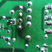
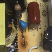
On close inspection of the three NMOS, I discovered that the gate of Q1 or Q2 is not working. Q3, whilst shows some physical damage, does seem to be working properly while testing with a DMM. The issue is Q8 broke off the board- I'm not sure if this was already damaged or was simply due to me trying to desolder it to test, and I can't seem to find documentation detailed enough to point me to what Q8 is supposed to be (NPN or a PNP).
I have found the service manual for this TV, but it has no detailed schematic for the SMPS (only a block diagram as below) and the circuit board layout only shows the top side of the board.

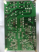
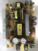
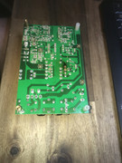
The board part number is PK101V0410I, or FSP291-4F01 - I have tried to contact some TV scrap sellers with this particular board in stock and also FSP to see if they can advise me on what Q8 should be, but I haven't heard back as yet.
I have tried to reproduce the schematic for this part of the board below- Q8 is there but I'm not sure if the device I picked (PNP) would be correct for this circuit.

Would anyone happen to have this board in their spares that they might be able to take a look, or advise me through their experience with this sort of MOSFET setup in a PFC circuit? My immediate thought was that it should be a PNP transistor, but the collector would then be connected to Vcc and I couldn't make sense of how this would work..
Kind regards
M
I have a L42X01A TV with a dead power supply - it blew the main fuse and I couldn't measure any shorts, but when I replaced the fuse, it blew again and left a mark between the drain and source of Q3 - which is in the PFC stage of the SMPS.
The PFC stage uses a NCP1653A which drives three 2SK3658 NMOS (Q1, Q2 and Q3) which has the drain and the source connected in parallel; the gate connection is different:
The gate of Q1 and Q2 are driven in parallel by a transistor (Q8) - it's either a PNP or an NPN; the emitter and collector are connected between Vcc and the gates of Q1, Q2.
On the other hand, Q3 is driven by a PNP transistor (Q11) with the emitter connected to the gate of Q3 and the collector connected to the source of Q1, Q2 and Q3.
I can see that Q8 and Q11 have their base connected together, and is driven by the drive pin of the NCP1653A.
On close inspection of the three NMOS, I discovered that the gate of Q1 or Q2 is not working. Q3, whilst shows some physical damage, does seem to be working properly while testing with a DMM. The issue is Q8 broke off the board- I'm not sure if this was already damaged or was simply due to me trying to desolder it to test, and I can't seem to find documentation detailed enough to point me to what Q8 is supposed to be (NPN or a PNP).
I have found the service manual for this TV, but it has no detailed schematic for the SMPS (only a block diagram as below) and the circuit board layout only shows the top side of the board.

The board part number is PK101V0410I, or FSP291-4F01 - I have tried to contact some TV scrap sellers with this particular board in stock and also FSP to see if they can advise me on what Q8 should be, but I haven't heard back as yet.
I have tried to reproduce the schematic for this part of the board below- Q8 is there but I'm not sure if the device I picked (PNP) would be correct for this circuit.

Would anyone happen to have this board in their spares that they might be able to take a look, or advise me through their experience with this sort of MOSFET setup in a PFC circuit? My immediate thought was that it should be a PNP transistor, but the collector would then be connected to Vcc and I couldn't make sense of how this would work..
Kind regards
M


